by Erin RobotGrrl | Dec 13, 2020 | News, Tech Logs
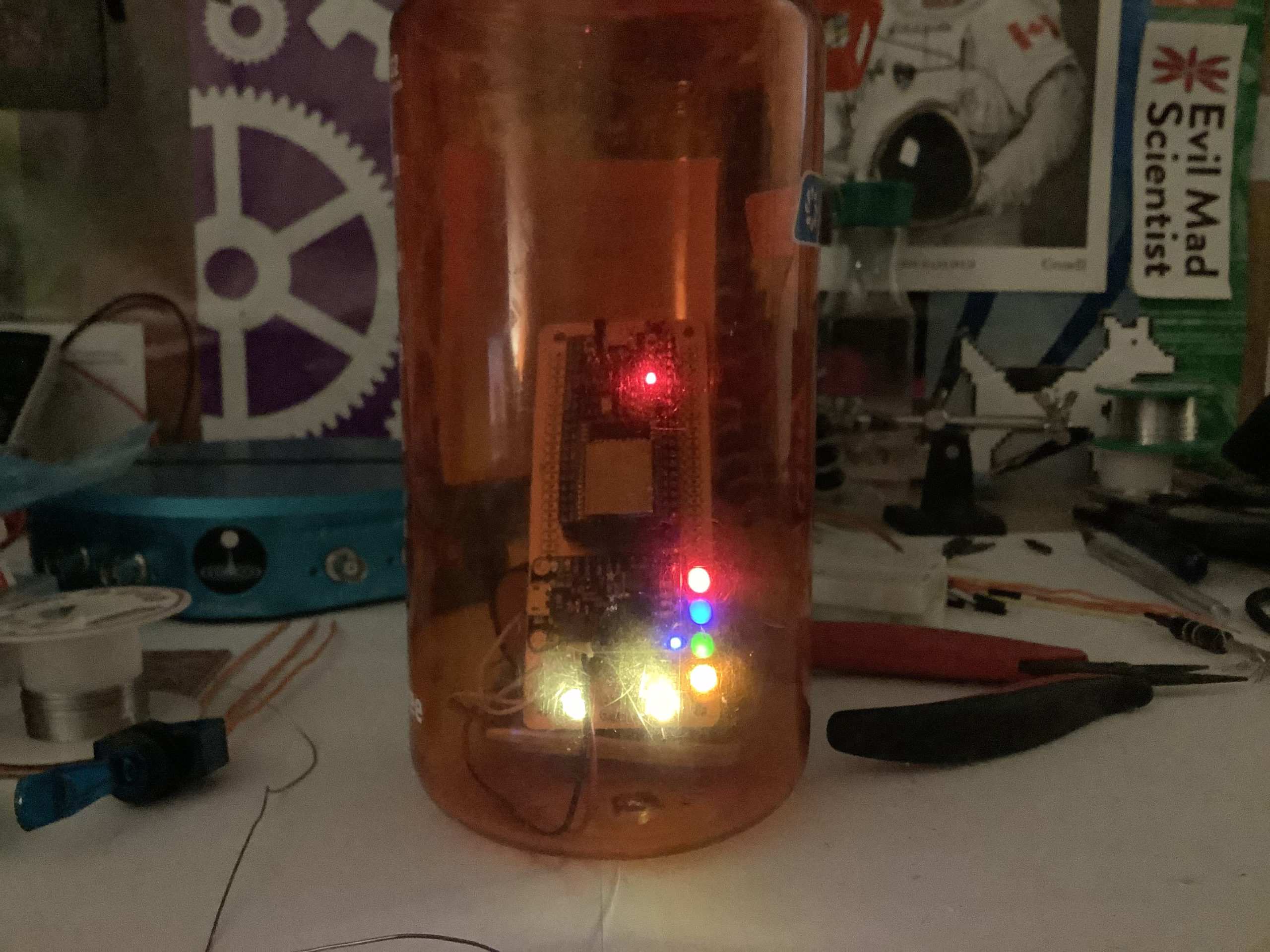
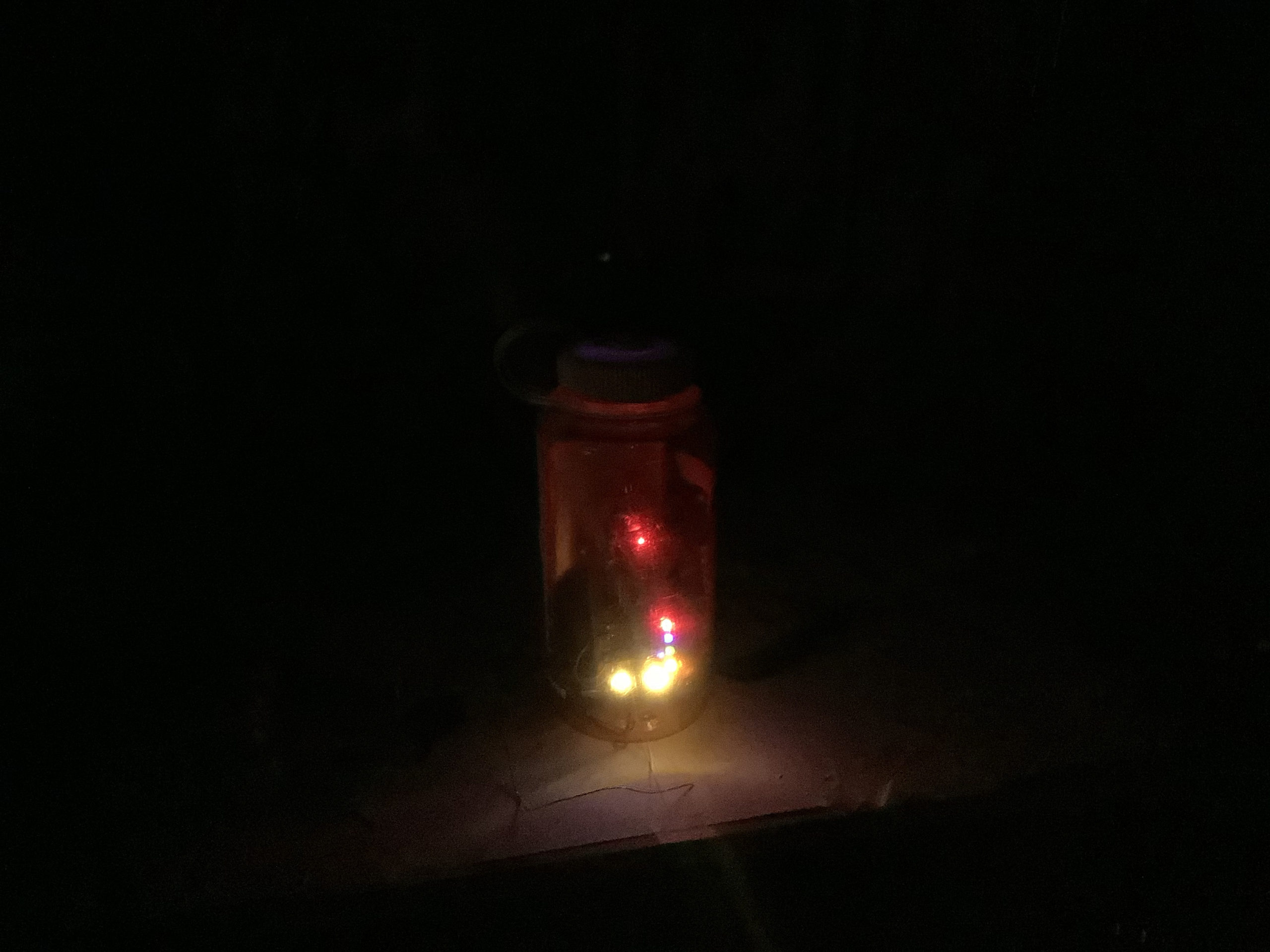
Basic blinking is done. It works! The analog value from the temperature sensor is received on serial monitor. Will need to remember in the future to go back and look at the actual formula used in the datasheet to go from this value to one in degrees Celsius. Before printing the pieces, work will have to be done on the 3D printer since it is experiencing an issue at some places on the build platform. Next step is back to the software, getting the AR draggable functionality working and ready to be merged with MQTT. Summary post is up on Patreon
here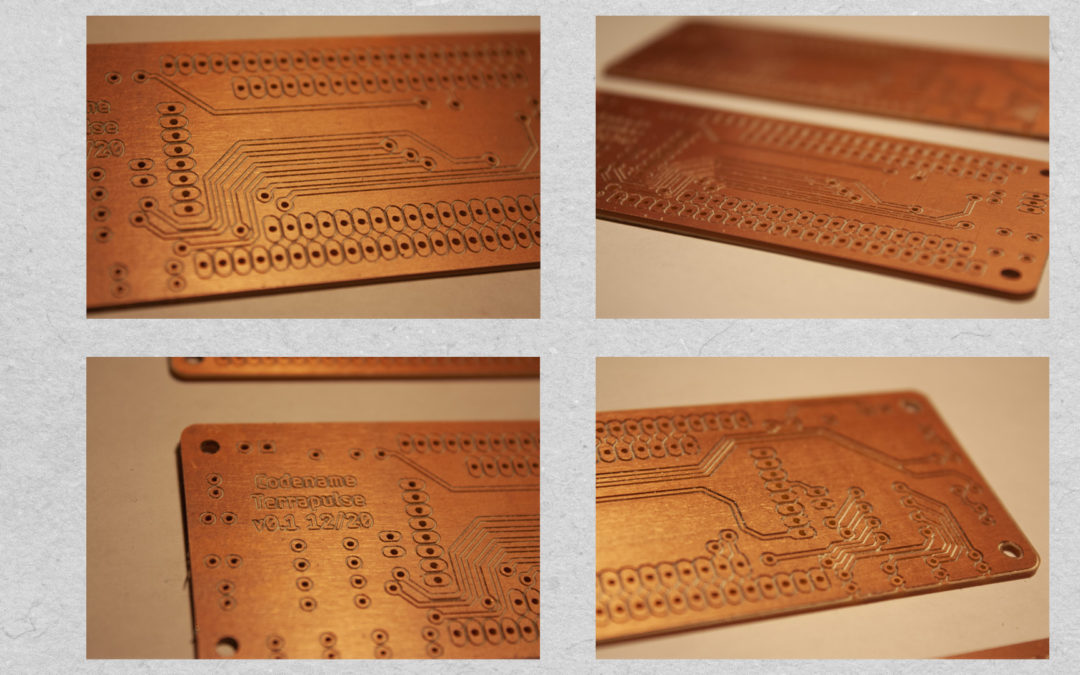
by Erin RobotGrrl | Dec 12, 2020 | News, Tech Logs
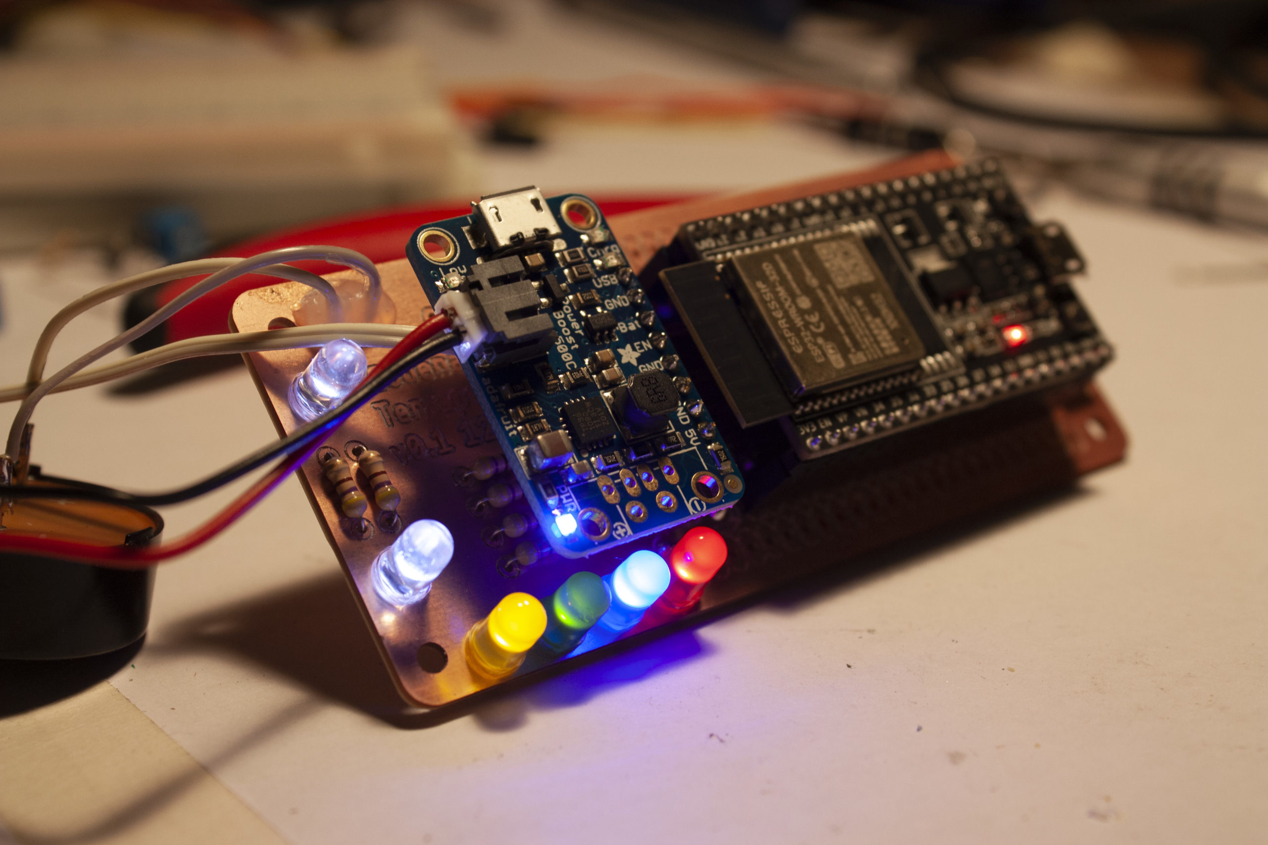
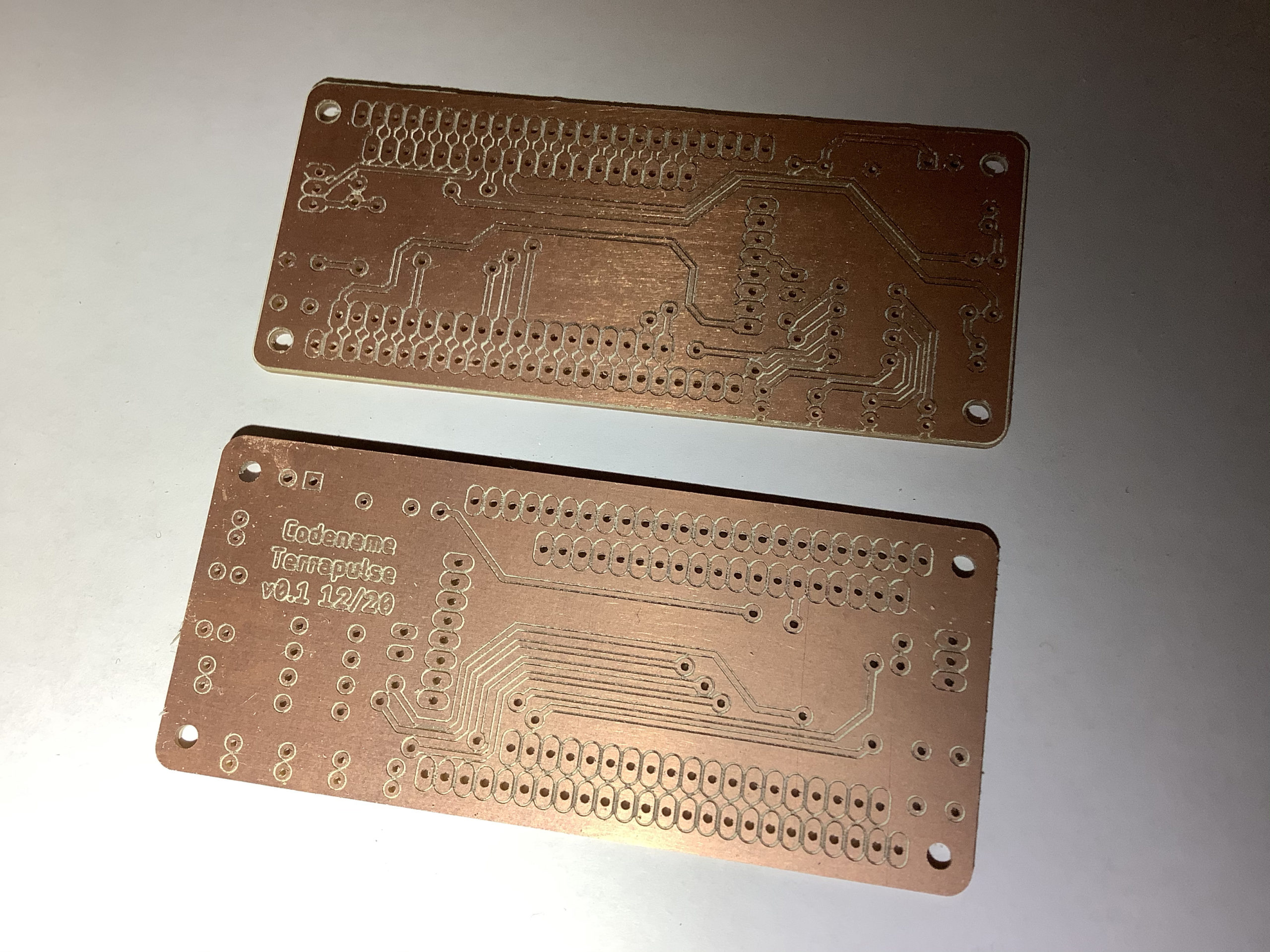
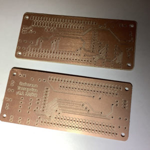
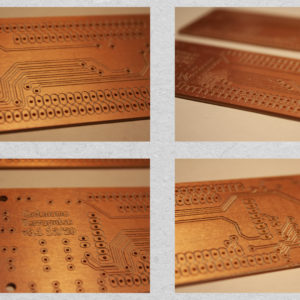
Milled the board, it’s done! Two of them actually – in case one of them failed. It was a long milling operation, taking up the entire space of the 4×6″ double sided copper clad piece. A 0.005″ v bit was used for engraving the traces, and a 1/32″ bit for the drills and outline. Decided to drill the holes on both sides (before flipping and after) and it helped to reduce the amount of time afterwards in post-processing by poking out some of the pieces that didn’t go through all the way. So that’s a great help. The thermal pads for the Gnd copper pour turned out well.
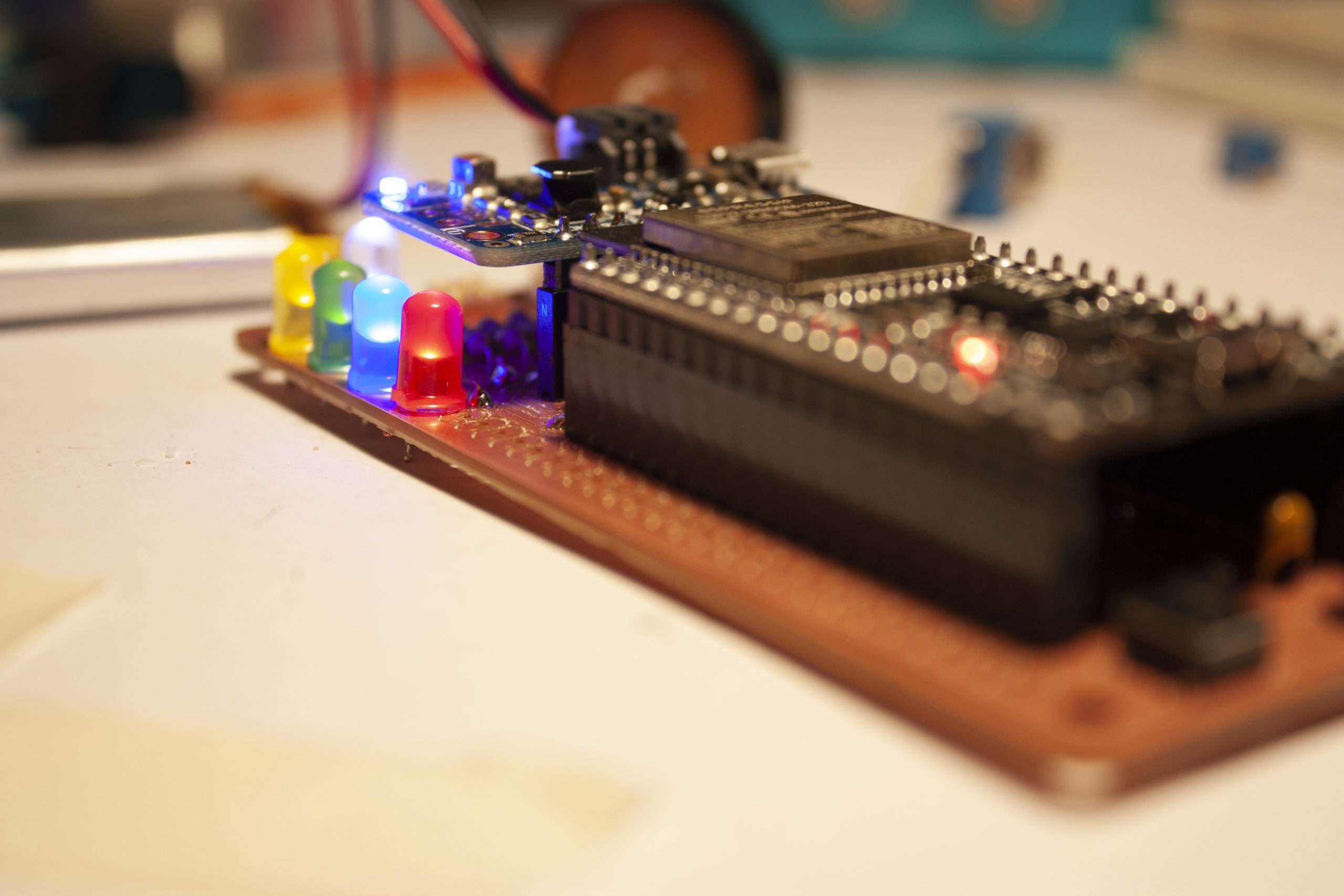
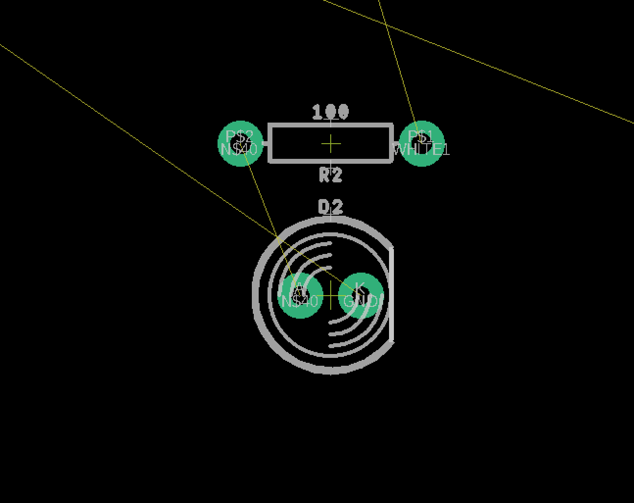
There were two mistakes found out on this iteration: forgot the resistor for the speaker, so this was wired in by hand after. White LED 1 on IO0 has the via going to the top layer through the pin pad. This doesn’t work since the holes are not through-plated. The solution was to jumper from the extra pad to the via, and the problem was solved. Hooray, the extra row of pads comes in useful for prototyping! Next step is coding more of the blinking patterns.
-
-
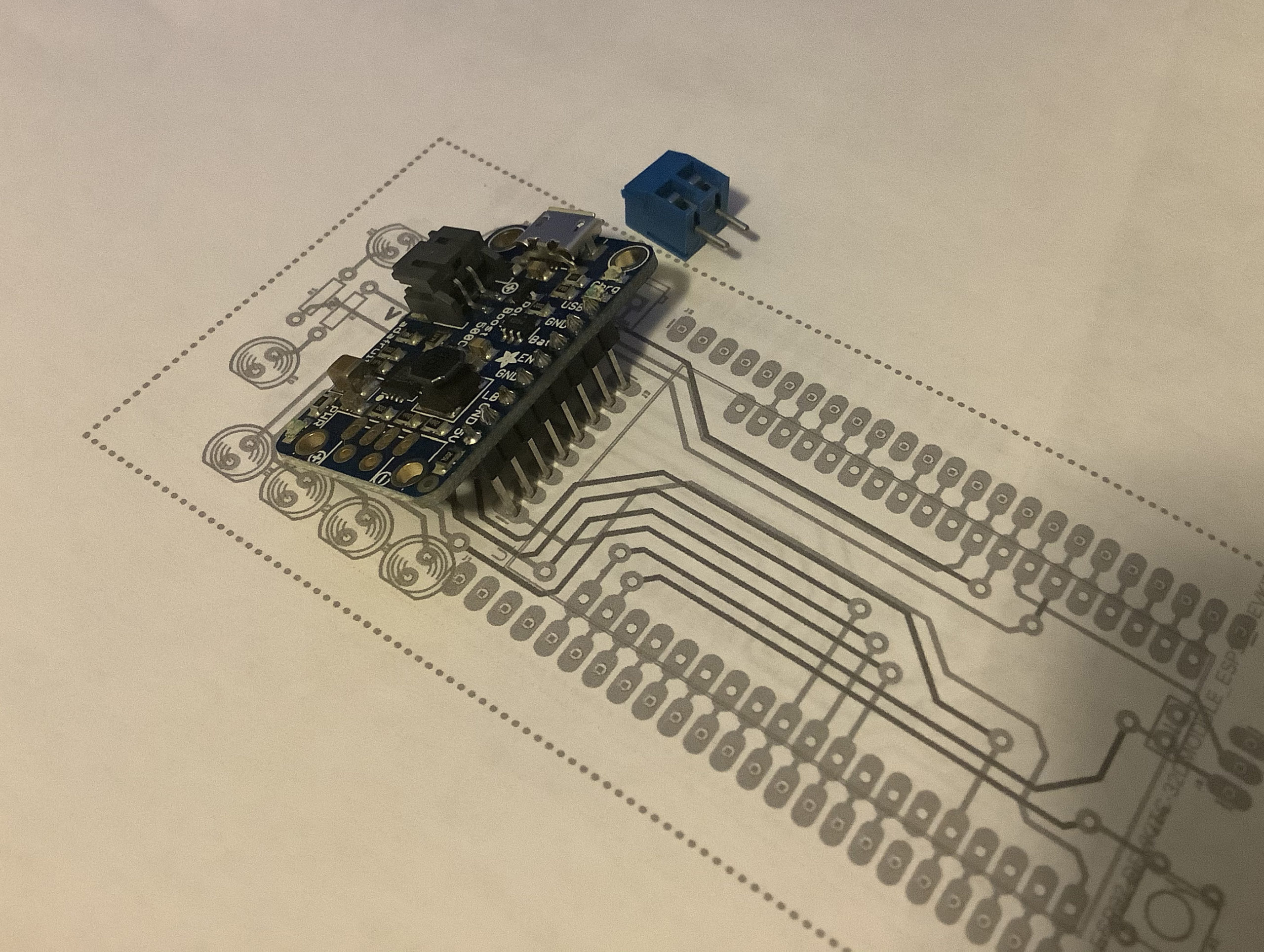
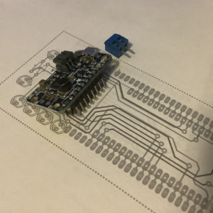
Paper test 1
-
-
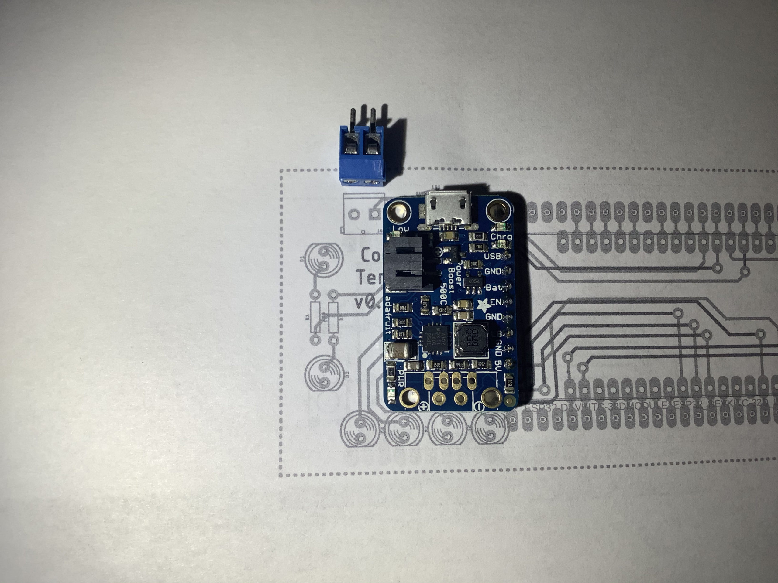
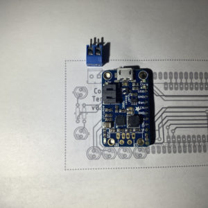
Paper test 2 after some adjustments
-
-
Boards milled
-
-
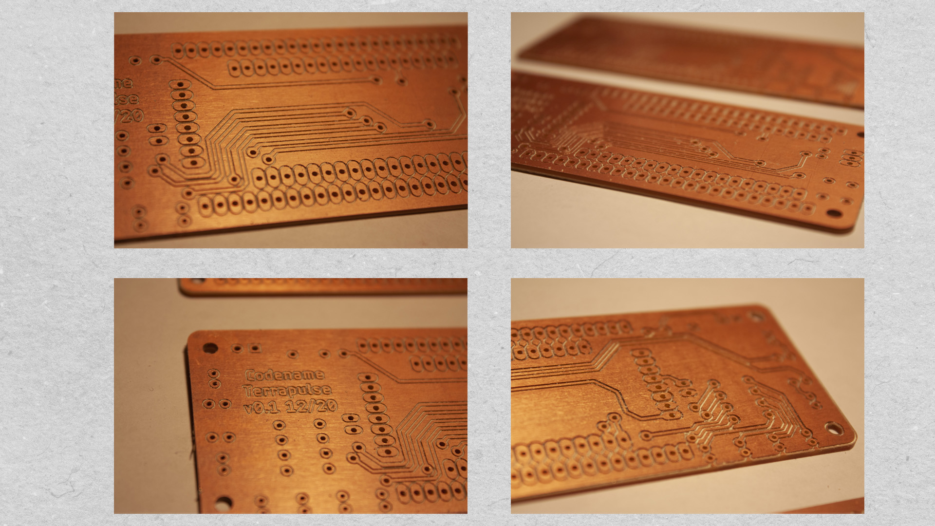
Closeup of boards
by Erin RobotGrrl | Dec 11, 2020 | News, Tech Logs
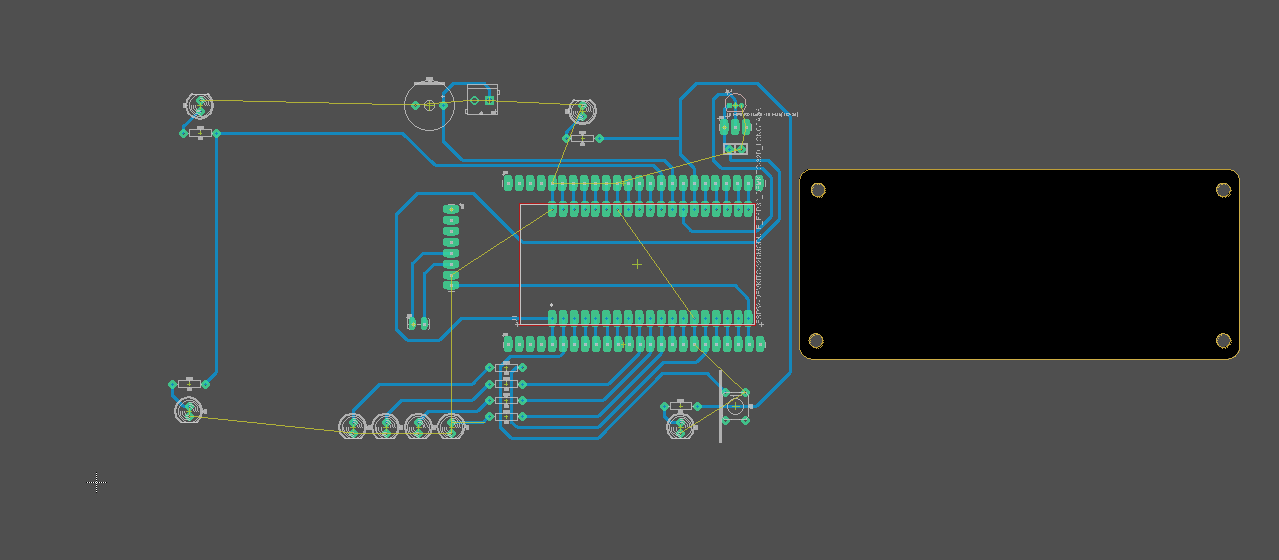
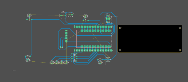
Board routing is done! Needed to do two iterations on it. The first iteration was routed without using the right dimensions on the outline. Oops. With the proper outline imported, everything needed to be placed closer together. Lesson learned: always import the proper outline (or close to it) as the first step. Alright, so the routing was completed fine. It is a 2 layer board with a copper pour on the back of the board. Tolerances for design for fabrication are 20 mils tracewidth, ample spacing at 10+ mils, and using longpads whenever possible. Vias are large like pads, so they can have a wire pass through them during the assembly stage. Next up is milling the board!

by Erin RobotGrrl | Dec 10, 2020 | News, Tech Logs
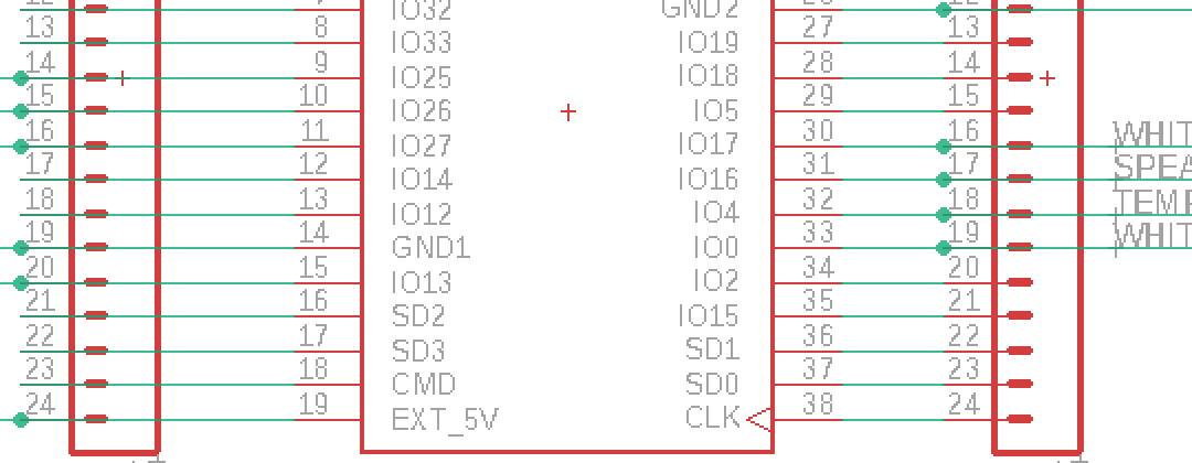
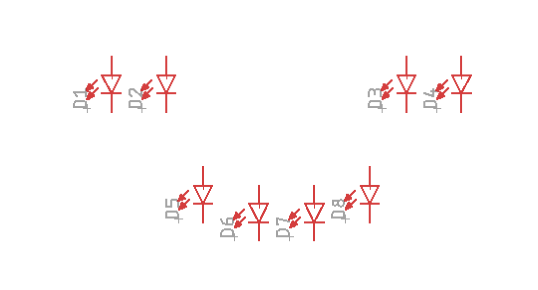
Schematic done for v0.1 of the sensor node! This is the most simplest design possible, with the barebones minimum. An ESP32 breakout, with headers to each side just in case, a reset switch, 6 LEDs, temperature sensor, speaker, and power boost board. All components are through hole at this moment in time. Pretty smooth sailing on this. Next step is to route the circuit board.
by Erin RobotGrrl | Dec 9, 2020 | News, Tech Logs
Basic code for the node to test input output functionality works. Two LEDs had to change pins as they were input only. PWM on ESP32 for LEDs is different than with the Arduino boards, that was interesting to learn about. Temperature sensor works, and analog input is 12 bit, so from 0 to 4095. Schematic is started. Next step is to complete the schematic, then board layout, and get the proper board outline with mounting holes into the design.