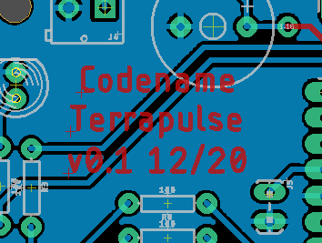
Tech Log #033: Circuit board v0.1 sensor node
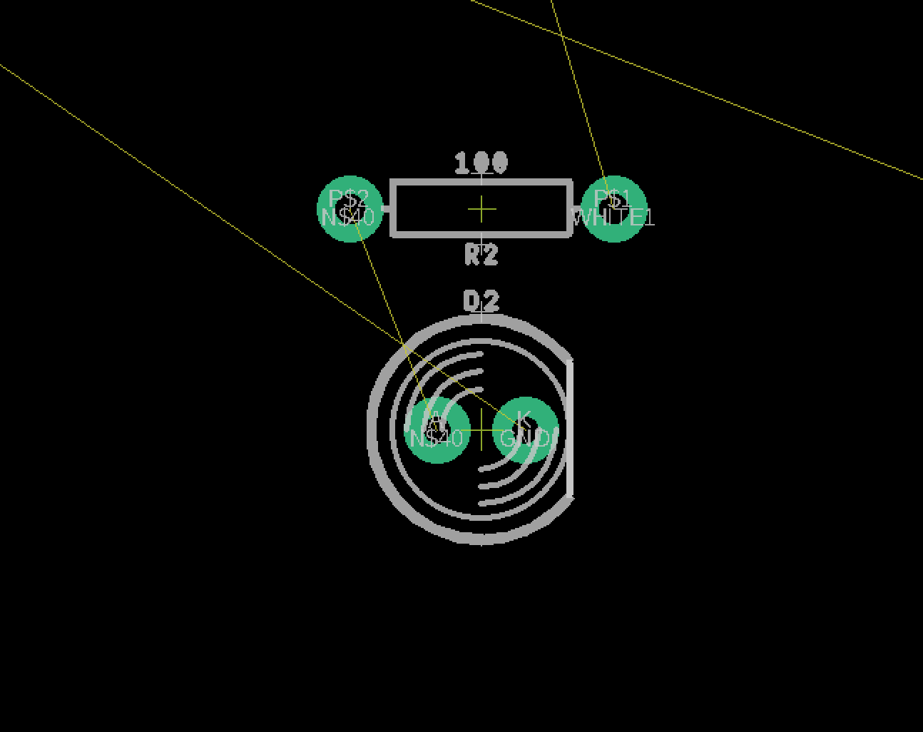
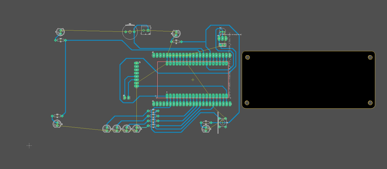
Board routing is done! Needed to do two iterations on it. The first iteration was routed without using the right dimensions on the outline. Oops. With the proper outline imported, everything needed to be placed closer together. Lesson learned: always import the proper outline (or close to it) as the first step. Alright, so the routing was completed fine. It is a 2 layer board with a copper pour on the back of the board. Tolerances for design for fabrication are 20 mils tracewidth, ample spacing at 10+ mils, and using longpads whenever possible. Vias are large like pads, so they can have a wire pass through them during the assembly stage. Next up is milling the board!